3. A Tour of the MultiGBASE-T1 SFP Hardware
Before learning how to configure and set up the device, let’s examine the device from all sides to understand all of its interfaces and status indicators.
3.1. LED Status Indicators
There are 2 visible LEDs on the device: LED1 and LED2, on the left and right, respectively, when looking into the connector
Link Speed |
Amber |
2.5G or 5G |
Green |
10G |
Link Status |
Amber LED |
Off |
Link Inactive |
Solid |
Link Active |
||
Flashing |
RX/TX activity |
||
Red LED |
Flashing |
Malformed Frame |
|
Solid |
MDIO Com Failure |
||
Blue LED |
Flash |
MACsec Enabled |
|
Both Red: Device Fatal Error |
|||
Both Blue: Device in bootloader |
|||
3.2. Connector Interfaces
3.2.1. Automotive Ethernet
This SFP module uses an H-MTD connection system with the following pin assignments.
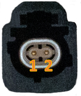
H-MTD Connector Pinout |
||
Pin # |
Label |
Description |
1 |
TRD+ |
Data transmit and receive, positive |
2 |
TRD- |
Data transmit and receive, negative |
For the mating H-MTD connector Reference USCAR-EWCAP Drawing Number 777-U-002-1-Z01
Important
The manufacturing of reliable Automotive Ethernet cables for 1Gbps speeds and above is complex and requires specialized equipment to insure the electrical characteristics are met to achieve a stable link with acceptable SQI. Modifying these cables or attempting to assemble cables without the proper knowledge and equipment can often lead to problems with establishing a link between two devices.
SFP Module Retention Feature
When the SFP module is inserted into an SFP slot, there is a locking mechanism for retaining the device in the slot. This locking mechanism can be released by the lever with a blue “ICS” label that rests above the H-MTD connector.
3.2.2. SFP+ Pin assignments:
PIN |
MultiG |
PIN |
MultiG |
|
1 |
GND |
11 |
GND |
|
2 |
TX_FAULT |
12 |
SFI_RX_C_N |
|
3 |
TX_DIS |
13 |
SFI_RX_C_P |
|
4 |
SDA |
14 |
GND |
|
5 |
SCL |
15 |
VCC |
|
6 |
GND |
16 |
VCC |
|
7 |
RATE_SELECT0 |
17 |
GND |
|
8 |
LOSS_OF_SIGNAL |
18 |
SFI_TX_C_P |
|
9 |
RATE_SELECT1 |
19 |
SFI_TX_C_N |
|
10 |
GND |
20 |
GND |
3.3. Device Configuration
This SFP is configured in software without the use of DIP switches or other mechanical interfaces.
3.3.1. SFP Configuration using Intrepid Hardware
If used with Intrepid hardware, the PHY settings can be changed using ICS Device Manager in the configuration screen seen below.
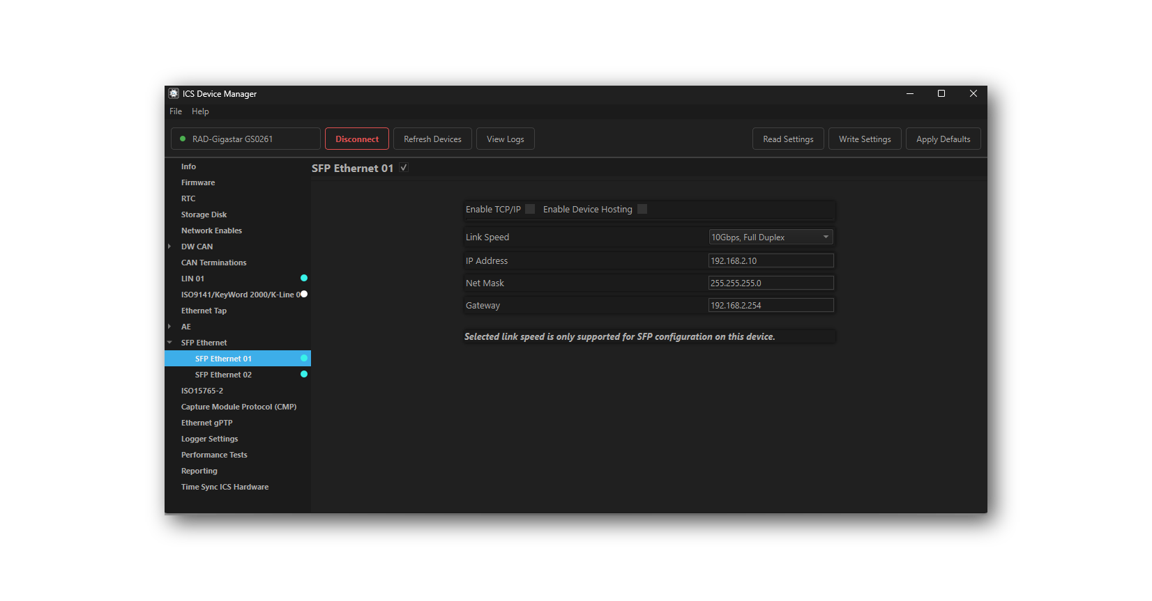
The following Intrepid devices support this configuration method:
The user guide of each device contains instructions on how to use ICS Device Manager to change the PHY settings in the ICS Device Manager section.
3.3.2. SFP Configuration using I2C
Configurations can also be made using I2C communication to the device and stored in non-volatile memory. The use of I2C for this and other purposes is explained in the next section.
3.4. I2C Communication
I2C communication with the SFP can be accomplished using 1 of 2 methods
Using a SFP host having exposed access to the I2C bus of the SFP module
Host the SFP module in an Intrepid product and use Vehicle Spy or the Intrepid API to send and receive I2C messages.
The following lists the Intrepid products capable of hosting this SFP as well as the I2C networks assigned to each SFP slot within VSPY.
Product |
VSPY I2C Network |
|
RAD-Gigastar |
SFP1 |
I2C 02 |
SFP2 |
I2C 03 |
|
RAD-Gigastar2 |
SFP1 |
I2C 01 |
SFP2 |
I2C 02 |
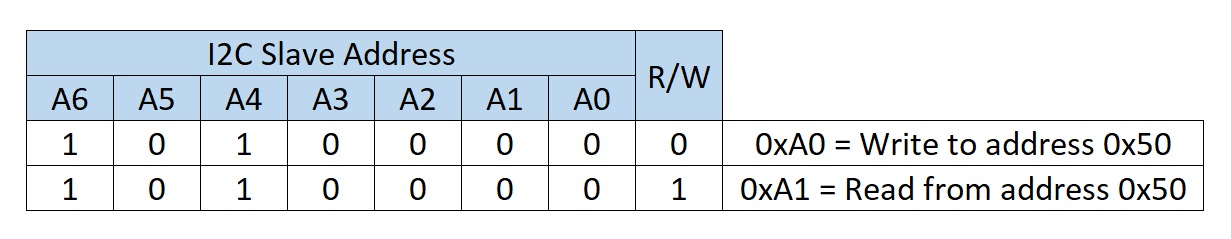
I2C Addressing
The first byte of an I2C message consists of a 7-bit device address appended with a read/write bit in the least significant position. It is worth pointing out that while I2C is limited to 7-bit device addresses, it is not uncommon for references to be made to 8-bit values that include the read/write bit. For example, below shows how 0xA0 refers to a write to device address 0x50 and 0xA1 refers to a read to that same address.
The SFP responds to the following 4 different I2C addresses
3.4.1. Address 0x50 - Read SFP MSA Table
The SFP MSA table is a 512-Byte table of which the contents are defined by SFP specification. The exact table contents are defined in the SFF-8472-Diagnostic_Monitoring_Interface specification.
MSA (Multi Source Agreement)
MSA stands for Multi Source Agreement. This is an agreement between multiple manufacturers on the standards for a given product. It is intended to ensure common functionality and operability across different suppliers and manufacturers.
A read of the MSA table could be done in VSPY with the following message.
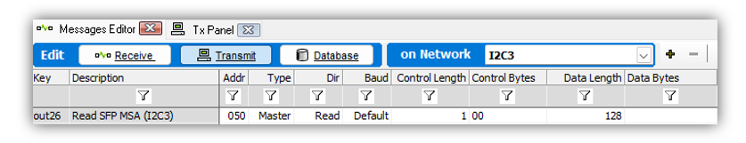
This starts at register 0 and reads the first 128 bytes from the table.
Byte Index |
Byte Description |
SFP-MV2112-A2 |
SFP-MV2221M-B1 |
SFP-MV3244 |
SFP-EN11100 |
SFP-AD1101 |
Byte 0 |
Identifier |
0x03 |
||||
Byte 1 |
Ext. identifier |
0x04 |
||||
Byte 2 |
Connector |
0xAF |
||||
Byte 3 |
Tranceiver |
0x00 |
0x10 |
0x00 |
||
Byte 4-10 |
Tranceiver |
0x00 |
||||
Byte 11 |
Encoding |
0x00 |
||||
Byte 12 |
BR, Nominal |
0x0A |
0x0A |
0x64 |
0x64 |
0x00 |
Byte 13 |
Rate identifier |
0x00 |
||||
Byte 14-17 |
Link Length (Fiber) |
0x00 |
||||
Byte 18 |
Link Length (Fiber) |
0x0A |
0x0A |
0x0F |
0x0F |
0x0F |
Byte 19 |
Link Length (Fiber) |
0x00 |
||||
Byte 20-35 |
SFP Vendor Name (ASCII) |
0x00,0x49,0x6E,0x74,0x72,0x65,0x70,0x69,0x43,0x53,0x20,0x20,0x20,0x20,0x20,0x20 -> “IntrepiCS______” |
||||
Byte 36 |
Transceiver |
0x00 |
||||
Byte 37-39 |
Vendor OUI |
0x00,0xFC,0x70 |
||||
Byte 40 |
Vendor PN (ASCII) |
0x53 |
0x53 |
0x53 |
0x53 |
0x53 |
Byte 41 |
Vendor PN (ASCII) |
0x46 |
0x46 |
0x46 |
0x46 |
0x46 |
Byte 42 |
Vendor PN (ASCII) |
0x50 |
0x50 |
0x50 |
0x50 |
0x50 |
Byte 43 |
Vendor PN (ASCII) |
0x2D |
0x2D |
0x2D |
0x2D |
0x2D |
Byte 44 |
Vendor PN (ASCII) |
0x4D |
0x4D |
0x4D |
0x45 |
0x41 |
Byte 45 |
Vendor PN (ASCII) |
0x56 |
0x56 |
0x56 |
0x4E |
0x44 |
Byte 46 |
Vendor PN (ASCII) |
0x32 |
0x32 |
0x33 |
0x31 |
0x31 |
Byte 47 |
Vendor PN (ASCII) |
0x31 |
0x32 |
0x32 |
0x31 |
0x31 |
Byte 48 |
Vendor PN (ASCII) |
0x31 |
0x32 |
0x34 |
0x31 |
0x30 |
Byte 49 |
Vendor PN (ASCII) |
0x32 |
0x31 |
0x34 |
0x30 |
0x31 |
Byte 50 |
Vendor PN (ASCII) |
0x2D |
0x4D |
0x2d |
0x30 |
0x20 |
Byte 51 |
Vendor PN (ASCII) |
0x41 |
0x2D |
0x41 |
0x20 |
0x20 |
Byte 52 |
Vendor PN (ASCII) |
0x32 |
0x42 |
0x31 |
0x20 |
0x20 |
Byte 53 |
Vendor PN (ASCII) |
0x20 |
0x31 |
0x20 |
0x20 |
0x20 |
Byte 54 |
Vendor PN (ASCII) |
0x20 |
0x20 |
0x20 |
0x20 |
0x20 |
Byte 55 |
Vendor PN (ASCII) |
0x20 |
0x20 |
0x20 |
0x20 |
0x20 |
Byte 56-59 |
Vendor Revision (ASCII) |
0xXX,0xXX,0xXX,0xXX |
||||
Byte 60-61 |
Wavelength |
0x00 |
||||
Byte 62 |
Unallocated |
0x00 |
||||
Byte 63 |
CC_BASE |
yy |
||||
Byte 64 |
Options |
0x00 |
||||
Byte 65 |
Options |
0x02 |
||||
Byte 66-67 |
BR max,min |
0x00 |
||||
Byte 68 |
Vendor SN (ASCII) |
0x53 |
0x53 |
0x53 |
0x53 |
0x53 |
Byte 69 |
Vendor SN (ASCII) |
0x31 |
0x32 |
0x34 |
0x36 |
0x37 |
Byte 70-73 |
Vendor SN (ASCII) |
0xXX,0xXX,0xXX,0xXX |
||||
Byte 74-83 |
Vendor SN (ASCII) |
0xXX,0xXX,0xXX,0xXX,0xXX,0xXX,0xXX,0xXX,0xXX,0xXX |
||||
Byte 84-91 |
Vendor Manufacturer Date (ASCII) |
0xXX,0xXX,0xXX,0xXX,0xXX,0xXX,0xXX,0xXX |
||||
Byte 92 |
Diagnostic Type |
0x00 |
||||
Byte 93 |
Enhanced Options |
0x00 |
||||
Byte 94 |
SFF-8472 Compliance |
0x00 |
||||
Byte 95 |
CC_EXT (8-bit sum of Bytes [64:94]) |
yy |
||||
Start of the Vendor-Specific Field |
||||||
Byte 96 |
MDIO Bridge I2C Address |
|||||
SFP-MV2112-A2 |
SFP-MV2221M-B1 |
SFP-MV3244 |
SFP-EN11100 |
SFP-AD1101 |
||
Byte 97 |
(Link Settings)
|
|||||
Byte 98 |
(MACsec, TC10, T1S, MultiG Link Speed)
|
0xFF (NA) |
0xFF (NA) |
|||
Byte 99 |
(PHY SerDes Link Speed)
|
0xFF (NA) |
0xFF (NA) |
|||
Byte 100 |
PLCA ID (10BASE-T1S) |
0xFF (NA) |
||||
Byte 101 |
Reserved |
0xFF |
||||
Byte 102 |
T1L Transmit Mode (10BASE-T1L) |
0xFF (NA) |
0x00 = 1.0V only |
|||
0x01 = 2.4V only |
||||||
0x02 = 1.0V capable of 2.4V |
||||||
Byte 103 |
Reserved |
0xFF |
||||
Byte 104 |
Device Status 1 (TC10) |
0xFF (NA) |
bit 0: TC10 sleep active (active low) |
0xFF (NA) |
||
bits 7:1: Reserved |
||||||
Byte 105 |
Device Status 2 |
bit 0: General PHY error |
||||
bits 7:1: Reserved |
||||||
Byte 106 |
PHY Test Modes |
0 = Normal Operation, Non-Zero = Test Mode # (e.g. 2 = Test Mode 2) |
||||
Byte 107-109 |
ICS_RESERVED |
0xFF |
||||
Byte 110-125 |
PCB Serial Number |
zz:zz:zz |
||||
Byte 126 |
Bootloader |
Value of 0xAA indicated the device is in the bootloader. |
||||
Byte 127 |
Vendor Overrides: |
bit 0: I2C MDIO bridge address override flag (inverted) |
||||
bit 1: Soft options override flag (inverted) |
||||||
Persistent Settings 1
Byte 97 of the MSA table holds the non-volatile PHY configuration and a couple SFP pin support flags. When the PHY settings are changed via I2C or neoVI Explorer, the new settings are saved to non-volatile memory to ensure the device boots back up into this state/configuration on next plug-in.
Value = 0 |
Value = 1 |
||
Bits 2:0 |
Reserved |
X |
X |
Bit 3 |
Link Mode |
Master |
Slave |
Bit 4 |
Auto Link Mode |
Disabled |
Enabled |
Bit 5 |
Auto Negotiation |
Disabled |
Enabled |
Bit 6 |
Support Rate Select |
Enabled |
Disabled |
Bit 7 |
Support TX Disable |
Enabled |
Disabled |
Persistent Settings 2
The following table describes the settings for Byte 98 of the MSA table which holds the states TC10, T1S, MACsec, and Multi-Gigabit Link Speed.
Bit 0: |
TC10 enabled |
0 = Disabled |
1 = Enabled |
||
Bit 1: |
MACsec enable |
0 = Disabled |
1 = Enabled |
||
Bits 3:2: |
MultiG Link Speed |
0b00 = Reserved |
0b01 = 2.5G |
||
0b10 = 5G |
||
0b11 = 10G |
||
Bit 4: |
T1S PLCA Enabled |
0: Disabled |
1 = Enabled |
||
Bit 5: |
T1S Multi ID Enabled |
0 = Enabled |
1 = Disabled |
||
Bit 6: |
T1S Collision Detect Enabled |
0 = Disabled |
1 = Enabled |
||
Bit 7 |
Reserved |
|
Persistent Settings 3
The following table describes the settings for Byte 99 of the MSA table which holds the state the PHY SerDes link speed.
0x00 = Default |
Supported speeds vary per device.
If a speed is not supported,
the device will use the default based on the link speed.
Supported speeds by device:
SFP-MV3244:
2500BASE-X
2.5GBASE-X (default for 2.5G)
5000BASE-R
5GBASE-R (default for 5G)
5G-USXGMII
10GBASE-R (default for 10G)
10G-USXGMII
SFP-EN11100:
1000BASE-X
1G-SGMII (default for 1G)
2500BASE-X
2.5G-USXGMII (default for 2.5G)
2.5G-OCSGMII
5GBASE-R
5G-USXGMII (default for 5G)
10G-USXGMII (default for 10G)
|
0x01 = 2500BASE-X |
|
0x02 = 2.5GBASE-X |
|
0x03 = 5000BASE-R |
|
0x04 = 5GBASE-R |
|
0x05 = 10GBASE-R |
|
0x06 = 5G-USXGMII |
|
0x07 = 10G-USXGMII |
|
0x08 = 1000BASE-X |
|
0x09 = 1G-SGMII |
|
0x0A = 2.5G-USXGMII |
|
0x0B = 2.5G-OCSGMII |
3.4.2. Address 0x51 - SFP Diagnotic Monitoring Interface
This functionality is not currently supported and will respond with 0xFF when read.
3.4.3. Address 0x40 - I2C MDIO Bridge
The registers of the PHY can be read and written using address 0x40.
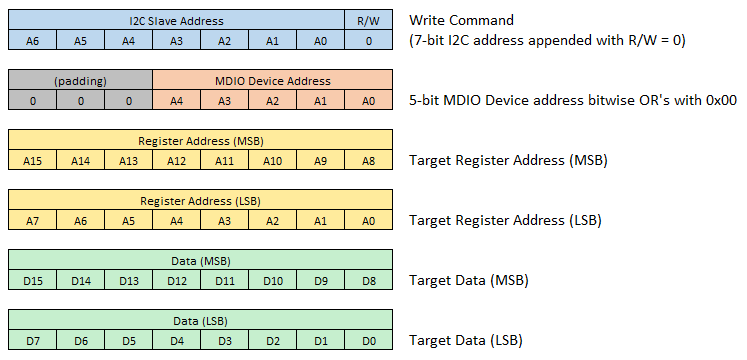
Writing to an MDIO Register
Writing to a register is done by sending the following sequence of bytes to the SFP over I2C.
This can be done in Vehicle Spy by sending an I2C message to the SFP hosted in a RAD-Gigastar.
The message editor creates the first byte using the address and R/W bit.
There are 3 “Control Bytes” consisting of the MDIO Address and the target address of the register.
The 2 “Data Bytes” is the value to be written to the target register.
Reading an MDIO Register
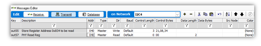
Reading an MDIO register over I2C is not an atomic transaction but requires a write command followed by a read command.
Step 1:
The address of the register to be read must first be sent to the slave in a write command. This is done by padding the MDIO device address with “001” (instead of “000”) which tells the slave that there is no data being written to a register, but to use the received address when responding to the next read command.
Step 2:
A read command is sent to the slave and a response is received with the contents of the register address written in step 1.
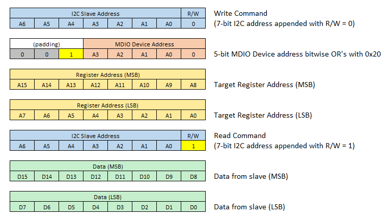
Sending the following messages will read the contents of register 0x0834.
Note
The MDIO Device Address logically OR with 0x20 to signify this is not a register write command, but a command to store the register address for the next read command. (same as padding with 001)
The read command has no control bytes
The number of data bytes in the read command determines how long the master will continue sending the clock to the slave and receive data.
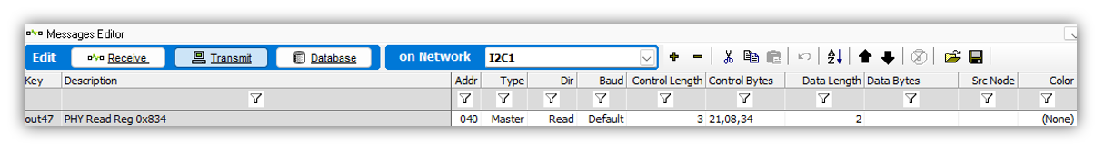
Alternative shortcut to reading an MDIO Register in Vehicle Spy
While there are valid reasons why a read from a device over I2C requires 2 operations, an I2C register read can be accomplished with a single message in Vehicle Spy. The following message in Vehicle Spy will generate the same 2 messages on the I2C bus as the previous I2C write example.
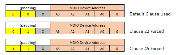
Forcing MDIO Clause 22 or Clause 45
For most devices, MDIO communication is accomplished using Clause 22 OR Clause 45. However, some devices may require both depending on the operation. The MDIO bridge defaults to one clause or the other based on the device, however, the clause used can be forced by the following operations performed on Control Byte 1.
Enable Force Clause: bitwise OR 0x40 with Control Byte 1
Force Clause 45: bitwise OR 0x80 with Control Byte 1
Force Clause 22: bitwise OR 0x00 with Control Byte 1
Control Byte 1 Examples:
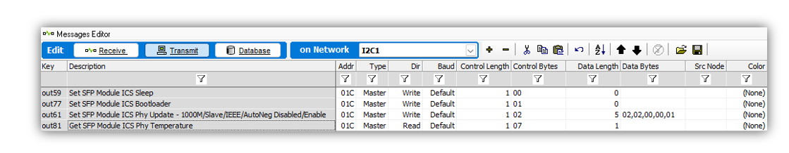
3.4.4. Address 0x1C - Intrepid Device Commands
Writing to address 0x1C with one of the following control byte values can be used to change the PHY configuration, mode of operation, as well as read back information such as PHY temperature and firmware version.
The SFP-MV2112 does not support MACsec or TC10.
Any MACsec or TC10 commands in the following table are not supported by the SFP-MV2112 or SFP-AD1101.
Control Byte |
Command Type |
Command |
|||
0 |
Write |
Enter Lower Power Mode |
Device will remain in low power until I2C message matching any of the 4 supported i2c slave addresses |
||
1 |
Write |
Jump to Bootloader |
SFP remains in bootloader expecting firmware update. Exit via power cycle. |
||
2 |
Write |
BASE-T1 PHY Configuration Command |
The PHY configuration can be changed by sending this control byte value based on this table. |
||
3 |
Write |
TC10 Wakeup |
Optional 1 byte argument |
0x00 = Trigger PHY via wake pin |
|
0x01 = Trigger wake via register access |
|||||
6:4 |
Reserved |
||||
7 |
Read |
Read PHY Temperature |
Value in Celsius |
||
8 |
Read |
Read SFP Minor Firmware Version |
|||
9 |
Read |
Read SFP Major Firmware Version |
|||
10 |
Read |
MACsec Update |
Accept settings and write MACsec configuration to the PHY |
||
11 |
Read |
Write MACsec Rule Settings |
|||
12 |
Read |
Write MACsec Map Settings |
|||
13 |
Read |
Write MACsec SecY Settings |
|||
14 |
Read |
Write MACsec SC Settings |
|||
15 |
Read |
Write MACsec SA Settings |
|||
16 |
Read |
Read Link Status |
bit 0: Link Status |
0 = Link down |
|
1 = Link up |
|||||
bit 1: Link Resolved |
0 = Not resolved |
||||
1 = Resolved |
|||||
bit 2: Duplex |
0 = Half duplex |
||||
1 = Full duplex |
|||||
bit 3: Mode |
0 = Slave |
||||
1 = Master |
|||||
bit 4: System Link Status |
0 = Link down |
||||
1 = Link up |
|||||
bits 7:5: Speed |
0b000 = 10Mbps |
||||
0b001 = 100Mbps |
|||||
0b010 = 1000Mbps |
|||||
0b011 = 2.5Gbps |
|||||
0b100 = 5Gbps |
|||||
0b101 = 10Gbps |
|||||
17 |
Read |
Read PHY Firmware Version
(SFP-MV3244/SFP-EN11100 only)
|
3-byte version of the form x.y.z |
||
25 |
Read |
Read PHY Signal Quality Indicator
(SQI)
|
SQI value reported by the PHY. |
SFP-MV2112: Range 0-15 |
|
All other devices: 0-7 |
|||||
26 |
Write |
Trigger TC10 Sleep Negotiation
With Link Partner
|
Sleep negotiation triggered regardless of the value written |
||
27 |
Read |
Read TC10 Sleep/Wake Status |
Byte 0 Current status |
bit 0: Wake status |
0 = Wake not received |
1 = Wake received |
|||||
bits 3:1 |
Reserved |
||||
bits 5:4: Sleep status |
00 = Normal |
||||
01 = Sleep |
|||||
10 = Sleep Failed |
|||||
11 = Reserved |
|||||
bits 7:6 |
Reserved |
||||
Byte 1 Interrupt status
(Bits cleared on read)
|
bit 0: Interrupt support |
0 = Interrupt byte supported
(active low)
|
|||
1 = Interrupt byte not supported
(all other bits are not valid)
|
|||||
bit 1: Wake received |
0 = Wake not received |
||||
1 = Wake received |
|||||
bit 2: Sleep received |
0 = Sleep not received |
||||
1 = Sleep received |
|||||
bit 3: Sleep failed |
0 = Sleep not failed |
||||
1 = Sleep failed |
|||||
bit 4: Sleep aborted |
0 = Sleep not aborted |
||||
1 = Sleep aborted |
|||||
bits 7:5 |
Reserved |
||||
28 |
Write |
10BASE-T1S PHY Configuration Command
(SFP-MC8670 only)
|
The 10BASE-T1S PHY configuration can be changed by sending this control byte value based on this table |
||
29 |
Read |
Read 10BASE-T1S PHY Status
(SFP-MC8670 only)
|
Byte 0 |
SQI in the range 0-7 |
|
Byte 1 |
bit 0 |
PLCA status |
|||
bit 1 |
TX collision |
||||
bit 2 |
TX jabber |
||||
bit 3 |
PLCA empty cycle |
||||
bit 4 |
RX in TO |
||||
bit 5 |
Unexpected beacon |
||||
bit 6 |
Unexpected carrier sense |
||||
bit 7 |
Decoding error |
||||
Byte 2 |
bit 0 |
Over temperature error |
|||
bit 1 |
Is coordinator (node ID == 0) |
||||
bit 2 |
Is PLCA enabled |
||||
bit 3 |
Is multiple IDs enabled |
||||
bits 7:4 |
Reserved |
||||
30 |
Write |
Load Default Settings |
Resets device settings to their default values.
Optional 1 byte argument.
|
bit 0: MACsec reset
(SFP-MV3244/SFP-MV2221M only)
|
0 = Do not reset MACsec settings |
1 = Reset MACsec settings |
|||||
bits 7:1 |
Reserved |
||||
31 |
Read |
Read General Status |
(SFP-MV3244/SFP-EN11100 only) |
bit 0: PHY Firmware Mismatch |
0 = No mismatch |
1 = Mismatch detected |
|||||
bits 7:1 |
Reserved |
||||
32 |
Write |
10BASE-T1L PHY Configuration Command
(SFP-AD1101 only)
|
The value of this control byte determines
the TX Amplitude(s) advertised during
auto-negotiation.
|
0x00 = 1.0V only |
If autonegotiation is not enabled,
the device will use 1V unless
the Data Byte Value is 0x01.
|
0x01 = 2.4V only |
|||||
0x02 = 1.0V capable of 2.4V |
|||||
33 |
Read |
Read 10BASE-T1L PHY Status |
(SFP-AD1101 only) |
bit 0: Link Status
(Same as 16.0)
|
0 = Link down |
1 = Link up |
|||||
bit 1: Link Resolved
(Same as 16.1)
|
0 = Not resolved |
||||
1 = Resolved |
|||||
bit 2: Mode
(Same as 16.3)
|
0 = Slave/Follower |
||||
1 = Master/Leader |
|||||
bit 3: TX Amplitude |
0 = 1.0V |
||||
1 = 2.4V |
|||||
bits 7:4 |
Reserved |
||||
34 |
Write |
Set Transceiver Code
Write up to 9 Data Bytes
|
Byte 0 |
Transceiver Code Override Enable |
0x00 = Disable Transceiver Code override |
0x01 = Enable Transceiver Code override |
|||||
Byte 1 |
MSA_TRANSCEIVER_CODE_BYTE_3 |
||||
Byte 2 |
MSA_TRANSCEIVER_CODE_BYTE_4 |
||||
Byte 3 |
MSA_TRANSCEIVER_CODE_BYTE_5 |
||||
Byte 4 |
MSA_TRANSCEIVER_CODE_BYTE_6 |
||||
Byte 5 |
MSA_TRANSCEIVER_CODE_BYTE_7 |
||||
Byte 6 |
MSA_TRANSCEIVER_CODE_BYTE_8 |
||||
Byte 7 |
MSA_TRANSCEIVER_CODE_BYTE_9 |
||||
Byte 8 |
MSA_TRANSCEIVER_CODE_BYTE_10 |
||||
35 |
Write |
Set PHY Test Mode
Write up to 3 data bytes
|
Byte 0 |
Test Mode Index |
|
Byte 1 |
Test Mode Precoder
(Not supported by current PHYs)
|
||||
Byte 2 |
Test Mode Jitter
(Supported by
SFP-MV3244/SFP-EN11100 only)
|
||||
Data Byte Encoding for 0x1C Control Byte 2
Data Bytes |
PHY Setting |
Data Byte Value |
|
Byte 0 |
Link Speed |
0x00 = 10Mbps |
Supported speeds vary per device.
If a speed is not supported,
the device will default to the lowest supported speed.
Supported speeds by device:
SFP-MV2112: 100M, 1000M
SFP-MV2221M: 100M, 1000M
SFP-MV3244: 2.5G, 5G, 10G
SFP-EN11100: 1000M, 2.5G, 5G, 10G
SFP-MC8670: 10M
SFP-AD1101: 10M
|
0x01 = 100Mbps |
|||
0x02 = 1000Mbps |
|||
0x03 = 2.5Gbps |
|||
0x04 = 5Gbps |
|||
0x05 = 10Gbps |
|||
Byte 1 |
Link Mode |
0x01 = Master |
All other values default to Slave |
0x02 = Slave |
|||
0x03 = Auto |
|||
Byte 2 |
Op Mode
(SFP-MV2112 Only)
|
0x00 = IEEE |
All other values default to IEEE mode |
0x01 = Legacy |
|||
Byte 3 |
Auto-Negotiation |
0bxxxxxxx0 = Disabled |
LSb state enables/disables feature |
0bxxxxxxx1 = Enabled |
|||
Byte 4 |
PHY Enable/Disable |
0bxxxxxxx0 = Disabled |
LSb state enables/disables PHY |
0bxxxxxxx1 = Enabled |
|||
Byte 5 |
PHY SerDes Link
(SFP-MV3244/SFP-EN11100 only)
|
0x00 = Default |
Supported speeds vary per device.
If a speed is not supported,
the device will use the default based on the link speed.
Supported speeds by device:
SFP-MV3244:
2500BASE-X
2.5GBASE-X (default for 2.5G)
5000BASE-R
5GBASE-R (default for 5G)
5G-USXGMII
10GBASE-R (default for 10G)
10G-USXGMII
SFP-EN11100:
1000BASE-X
1G-SGMII (default for 1G)
2500BASE-X
2.5G-USXGMII (default for 2.5G)
2.5G-OCSGMII
5GBASE-R
5G-USXGMII (default for 5G)
10G-USXGMII (default for 10G)
|
0x01 = 2500BASE-X |
|||
0x02 = 2.5GBASE-X |
|||
0x03 = 5000BASE-R |
|||
0x04 = 5GBASE-R |
|||
0x05 = 10GBASE-R |
|||
0x06 = 5G-USXGMII |
|||
0x07 = 10G-USXGMII |
|||
0x08 = 1000BASE-X |
|||
0x09 = 1G-SGMII |
|||
0x0A = 2.5G-USXGMII |
|||
0x0B = 2.5G-OCSGMII |
Data Byte Encoding for 0x1C Control Byte 28
This Control Byte is only supported by the SFP-MC8670 and is used to configure 10BASE-T1S PHY settings.
Data Byte |
10BASE-T1S PHY Setting |
||
Byte 0 |
PLCA Max Burst Count |
||
Byte 1 |
PLCA Burst Timer |
||
Byte 2 |
PLCA Max Number of Nodes |
||
Byte 3 |
PLCA Local Node ID |
||
Byte 4 |
PLCA Transmit Opportunity Timer |
||
Byte 5 |
PLCA Enable |
||
Byte 6 |
PLCA Collision Detection Enable |
||
Byte 7 |
CSMA Fallback Enable |
||
Byte 8 |
Multiple ID Enable Mask |
bit 0 |
Enable multi ID 0 |
bit 1 |
Enable multi ID 1 |
||
bit 2 |
Enable multi ID 2 |
||
bit 3 |
Enable multi ID 3 |
||
bit 4 |
Enable multi ID 4 |
||
bit 5 |
Enable multi ID 5 |
||
bit 6 |
Enable multi ID 6 |
||
bit 7 |
Reserved |
||
Byte 9 |
Multi ID 0 |
||
Byte 10 |
Multi ID 1 |
||
Byte 11 |
Multi ID 2 |
||
Byte 12 |
Multi ID 3 |
||
Byte 13 |
Multi ID 4 |
||
Byte 14 |
Multi ID 5 |
||
Byte 15 |
Multi ID 6 |
||
Example 0x1C Command Messages in Vehicle Spy
The following shows example messages for various 0x1C commands using Vehicle Spy with the SFP hosted in a Intrepid device (e.g. RAD-Gigastar or RAD-Gigastar2)